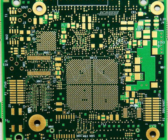

What Are HDI PCBs?
HDI pcb is an electronic design that incorporates more interconnections in a smaller space than a traditional circuit board. This miniaturization can make it ideal for applications requiring higher performance without sacrificing board size.
High density interconnect PCBs are a popular choice for complex electronics such as mobile / cellular phones, digital cameras, and 4/5G network communications. They also work well in aerospace applications.
Miniaturization
Miniaturization of electronic devices is a growing trend in the industry. This is driven by a number of technologies, including 5G networks and artificial intelligence. Moreover, these trends are also accelerating manufacturing processes to a new level.
High-density interconnect (HDI) boards are a popular choice for many industries, including electronics, medical, aerospace and military. They are especially suitable for products that require low power consumption and good performance, as well as those in harsh environments.
Using HDI technology, you can reduce the overall size of your circuit board, making it easier to place smaller components. This allows you to increase your interconnections, and it also means that your signal transmissions are faster and more reliable.
Additionally, fewer components and shorter trace widths mean that the resistance that your signals encounter is significantly reduced. This decrease in resistance is achieved by the short distances between the microvias and pads, as well as by a lower dielectric thickness.
The combination of these features means that you’ll have a smaller board, which will save space and increase the efficiency of your design. Furthermore, you’ll have a higher output with less power consumption, which makes the overall cost of your product less expensive.
The manufacturing process for a HDI board requires a number of unique steps that use specific equipment. These can include sequential lamination cycles, laser drills and other specialty tools. It is important to choose a CM or manufacturer that has these resources available. This will ensure that you receive the highest quality product possible.
More Interconnections
HDI PCBs contain more interconnections than standard circuit boards, allowing them to fit more components on one board. This increases the design flexibility of the product and enables designers to place smaller components closer together for better performance.
A layered HDI PCB typically contains multiple types of vias, through-holes or microvias to connect layers and allow signals to flow through them easily. These features occupy minimal space and can be drilled into the circuit board with lasers, CNC machine tools or other techniques.
Buried Vias: These are a type of via hdi pcb that goes through two internal layers of a multi-layer HDI PCB, but cannot be seen from the outside. This technique requires a separate drill file and is typically used for connecting the top and bottom layers of a board.
Through-Holes: These are holes with a diameter of less than 150 microns that can be drilled into the top and bottom layers of a high-density PCB. These holes are most commonly implemented to connect one layer to the adjacent layer and can be drilled with a laser or a CNC machine.
A high-density PCB can be made with different number of through-holes, vias and microvias depending on the functionality of the product. The type and amount of these features will affect the cost of the product. For example, a 2-n-2 layout will be more complicated than a 1-n-1 and will be more expensive to produce. This is because the process of lamination will require sequential laminations that can increase costs. Also, the stackup height and the number of layers will impact cost.
Better Performance
HDI pcbs offer better performance in comparison to traditional PCBs. This is because of their finer lines, closer spaces, and more dense wiring. This can improve signal transmission and reduce EMI.
Another benefit of HDI boards is that they are less expensive than standard PCBs. Because of their finer line structure, HDI boards can reduce the number of layers needed in a PCB design, which can help save money.
Moreover, they have a higher glass transition temperature (Tg), which can help them withstand thermal shock. This can also increase their reliability.
These benefits are why many electronic manufacturers choose HDI pcbs to manufacture their products. They are a common option for mobile/cellular phones, touch screen devices, laptop computers, digital cameras, 4/5G network communications, and military applications.
The best thing about HDI pcbs is that they offer superior performance without any extra costs. They can be used as all-in-one circuit boards, which makes them ideal for hdi pcb any company that wants to maximize its profit margin.
It is important to note that designing HDI boards requires more expertise than other types of PCBs. In addition, there are several manufacturing steps that need to be completed in order to produce an HDI board.
One of the most challenging steps is burying and plugging holes. This step must be performed correctly to ensure the integrity of the final product.
A failure to properly bury or plug holes can lead to uneven board borders, inconsistent dielectric thickness, pitted pads, and other problems. This means that manufacturers must be extremely careful during the process.
Ultimately, the best way to ensure that you get a high-quality HDI pcb is to find a reliable manufacturer. The quality of the products you get from your PCB supplier will have a large impact on your overall cost.
More Reliability
The reliability of a PCB is crucial to the performance of an electronic device. If the PCB fails, the device will no longer function as it was designed. The greater the reliability of the PCB, the more likely it is to last a long time in its intended environment.
HDI (High Density Interconnect) technology is a popular choice in many electronics products because of its ability to reduce size and weight without sacrificing reliability or signal integrity. The high-density nature of these circuit boards enables designers to place more components on the board while using less space, which can result in lower overall costs and faster shipping times.
This technology allows for smaller traces and vias, as well as a lower aspect ratio on microvias, which means better plating and overall board reliability. Additionally, the near-pad technique for placing vias eliminates any potential issues related to drill wander – which is where a component comes off the pad and touches another trace, creating a break-out channel in the case of a through hole that deviates from the intended drill hit location.
Moreover, the use of thinner prepreg material in HDI technology can also improve heat transfer across the board. This can help keep the temperature under control and increase board lifespan.
Generally, the main applications for HDI technology include medical devices such as cardiac pacemakers and implanted devices, wearable devices, digital cameras, avionics and smart munitions, 4/5G network communications, mobile phones and laptop computers. These devices require small packages that can deliver super transmission rates, which HDI PCBs provide.
Lower Cost
HDI PCBs are an excellent choice for many applications because they can reduce overall costs. They can be manufactured with fewer layers and smaller sizes than traditional boards, so manufacturing processes can be more efficient. They also have design efficiencies that can help with faster production times and shorter lead times to market.
Low Cost
The lower cost of HDI circuit boards is mainly due to the fact that they use materials with less dielectric constants and coefficients of thermal expansion than standard PCBs. This allows them to be more durable and to function better in extreme temperatures.
In addition, they can be used in applications where space is limited or weight is a concern. This can make them a great option for applications like smart devices, industrial equipment, and military technology.
Higher Connectivity Density
HDI circuit boards can have a higher electrical connections pad density than traditional boards, which means that they require a smaller area to connect all of the components on the board. This can also improve routing density and make it easier for ICs to be connected to each other.
This makes it easy for your products to function, so they’re more affordable to manufacture. They’re also ideal for high-speed telecommunications and military applications, because they can transmit signals more efficiently.
Another factor that can contribute to the lower cost of HDI pcbs is their high reliability. This is because they use microvias that have a smaller aspect ratio than traditional through-holes, which can increase their lifespan and ensure that your product performs correctly for longer periods of time.
If you’re looking for an HDI pcb that will offer you all of these benefits, then it’s important to work with a company that has experience in a wide range of different industries and can offer a comprehensive design and manufacturing service. This way, you can rest assured that your products will work well for years to come and that you’ll be able to save money in the long run.